|
The 80c196kc family's on-chip peripheral set includes a Pulse Width Modulator
(PWM) for generating a pulse train of varying width, which can be filtered to
generate analog voltages. This can be used to generate sine waves and even more
complex waveforms by periodically changing the PWM value.
Note that different members of the 8096 family may have 1, 2, or 3 PWM
generators, and may implement them in different manners. This application note
is specific to the PWM generator in the 8096 and 80C196KC/KD families of parts,
not the HSI/O module's PWM mode, or the PWM generator of the 80C196MC, although
similar applications may be possible with these parts. |
1)
80C196KC 의 기능
☞ 256 byte RAM
☞ 232 byte
register file
☞ Power
down /idle mode ☞ 16
bit watchdog Timer
☞ Serial
UART
☞ 8bit/16bit
bus width
☞ HOLD/HOLDA bus
control ☞ 5
EA 8 bit I/O Port
☞ 3EA
PWM output ☞
28 interrupt source
☞ 16
EA interrupt Vector ☞ 4
EA 16 bit software timer
☞ timer
2 cap, inc/dec counting function ☞ sample/hold-function
8/10 bit A/D convertor
☞ PTS(peripheral transactoin
(2)
80C196KC

3) How
to assemble the 80196kit
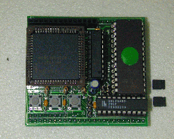
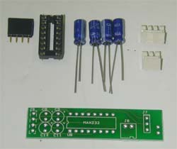
1.
Check
the components with the list.
2. Devide
the main board and the communication board.
.  ----> ----> 
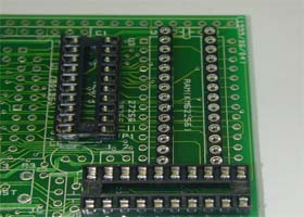
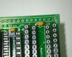
3. Put
the IC socket into then solder it. Remain the 64pin PLCC socket for the last
soldering.
The
IC socket which has a groove on top should head to No. IC1 side.
Put
the 27C256 into on top of the 62256 by the round socket. Make
the the middle of the 80c196 socket then solder it.
 
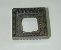 
참고: 64핀 PLCC 타입은 중앙에
있는 부분을 위에 있는 사진과 같이 홈을 만든 다음에 소켓을 끼우고
납땜을 수행하면 될 것이다. 중앙에 콘덴서와 크리스탈을 납땜하기
위해서 하는 작업임을 명심하자.
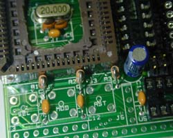
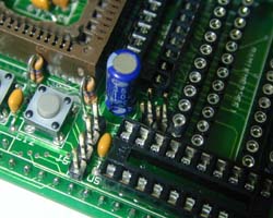
4. Solder
the Christal(Y1) / 20pF ceramic condenser 2EA / Condenser / 104 Condenser in the
middle of the
80c196 socket. Solder the 4.7K resistor 3EA/ 104
Condenser/ 10uF Electrolytic condenser.
Caution) 10uF electrolytic
condenser has the polarity, the long lead and black side is (+).
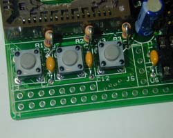
5. Solder
the 3 switches(Push SW S1, S2, S3)
Solder the JP1 / J5
104
Solder the condenser 3EA / Header pin female.
6. solder header pin male(J2:
for LCD ), header pin female(JP1, Serial port J5 board).

5. Solder header pin female(J1,
J3, J4). it is extension port.


/*
Solder header pin male(J1, J3, J4) as shown in fig
*/
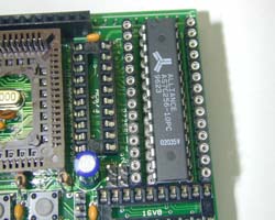
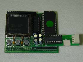
Put
the IC from the 62256. Put
the 2 jumpers into the JP1 vertically.
6. Put the IC socket U4
for 61256 RAM. put the U1(80c196kc), U2(74HC573), U4( 27C256
ROM),
U5(16V8). put the jumper socket in the JP1 header pin .
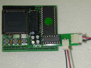
7. Making
the communication board(Max232)
(solder the header pin female J6, IC socket U6, connector maleJ7, J8 and
condencer 22uF 4EA)
 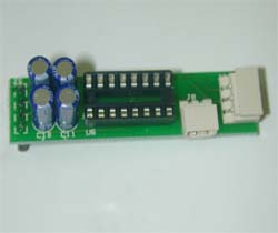
8. connect the
communication board with 80c196kc main board
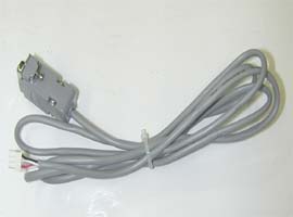
9. Make a
communication
cable.
  
 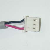 
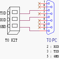
** 9 pin connector : No2 pin(Red), No3 pin(White), No5
pin(Black).
10.Put
the power into. Be careful the direction. If the polarity is changed, the board
will be out of order.
You should check the memory at the communication
situation and download one file for make sure

|


